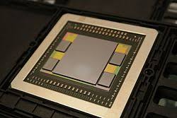
Modern SoC designs need many interconnects for good performance. Cache coherent and non-coherent interconnects work together. It’s important for SoCs to have a good mix of both.
Accelerators and peripherals in SoCs don’t need cache coherency. But sharing memory and I/O is crucial so the processor has access to up-to-date data without leaving the chip. Arteris says its non-coherent FlexWay interconnect IP and Ncore cache coherent NoC IP work well together.
The latest version of its cache-coherent NoC IP works with various processor IPs, including RISC-V and Armv9 Cortex. Arteris has validated the Armv9 Cortex processor IP for its Ncore cache coherent interconnect IP. The validation system boots Linux on a multi-cluster Arm design and tests critical cache coherency cases.
It supports many protocols, including CHI-E, which is associated with the latest Armv9 processors. Other protocols are CHI-B and ACE coherent, plus ACE-Lite and AXI* IO coherent interfaces. This allows designers to use older architectures and save money.
Interconnect IP is now ISO 26262 certified by the certification agency exida. The Ncore version of Arteris’ interconnect design is certified, which means it is ready to use with ISO 26262 certification. The software side of Ncore has a straightforward user interface flow that starts with chip specifications and ends with generating RTL. NCoR maintains a database of inputs for SoC architectures, making managing specifications easier. Charles Janac, Arteris’ CEO, says that modern electronics’ complexity presents challenges for SoC designers.
Ncore can connect any processor using any protocol and topology. It supports different connectivity options for adaptable use in various applications across different markets like automotive, industrial, communications, and enterprise computing.
TrendForce predicts that HBM3 will transition to HBM3e in 2024 and SK hynix is leading with HBM3e validation this quarter. SK hynix is currently the primary supplier of HBM3 memory chips for Nvidia’s H100 AI solutions. Samsung has received certification for AMD’s AMD MI300 series AI accelerators, a significant breakthrough for the memory supplier. AMD’s AI accelerators are expected to scale up later this year. Micron is catching up by launching HBM3e for Nvidia’s H200 GPUs by the end of Q1 2024, with shipping starting in Q2 2024. Micron largely missed the HBM opportunity.
SK hynix is ahead of Micron and Samsung in HBM technology since 2013. SK hynix partnered with AMD to introduce HBM memory. Samsung developed the HBM2 device in 2015, two years after SK hynix.
The rivalry between SK hynix and Samsung is not just about being the first. Samsung uses non-conductive film technology for HBM chips while SK hynix uses mass reflow molded underfill method to address NFC limitations.
SK hynix has 60-70% yield rates for HBM3 production, while Samsung only has 10-20%. The MUF process improves heat dissipation and production yields by injecting and hardening liquid material between silicon layers. SK hynix worked with Namics and Nagase to adopt this technique and became the first to supply HBM3 chips to Nvidia. Samsung is reportedly in contact with MUF material suppliers but plans to stick to NFC technology for upcoming HBM3e chips. Industry observers note that Samsung’s MUF technology won’t be ready until 2025, so they may use both NFC and MUF techniques.